Likes
Gallium selenide crystals are used in semi-conductors, ultra-thin nanomaterials and other applications due to their unique electronic and optical properties. The GaSe crystals are layered and soft, and they take days to grow, which makes it difficult to fully explore their applications and advance future technologies.
To compensate for the time difference, an international research team devised a method to produce crystals of comparable quality in just 5 minutes. The study was published on December 26th, 2021, in the Nano Research journal.
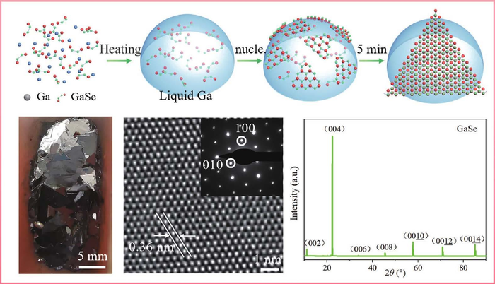
 A liquid-metal-assisted chemical vapor deposition method is proposed to rapidly synthesize centimeter-sized GaSe crystals of high crystal quality, which shows good performance of photodetector. Image Credit: Nano Research.
"In this paper, we propose an ultrafast crystal growth process with low energy consumption and capability of producing crystals of excellent quality. We also demonstrate that large-sized GaSe crystals—half to one centimeter long—can be obtained within the short period of five minutes." said Yumeng Shi, Study Co-Corresponding Author and Professor, Engineering Technology Research Center for 2D Material Information Function Devices and Systems of Guangdong Province, Shenzhen University.
Yumeng Shi is also a professor at the International Collaborative Laboratory of 2D Materials for Optoelectronics Science and Technology of Ministry of Education, Institute of Microscale Optoelectronics at Shenzhen University.
GaSe crystals are typically grown using chemical vapor transport, in which the starting chemical components react with a solution, reconfiguring their constituents into liquid, gas and solid phases, which settle out as crystals once properly separated, usually by temperature.
They can also be grown using the vertical Bridgman technique, which uses the same temperature controls but involves a seed crystal that shares the geometry of the crystal to be grown. As the material is produced, it forms its own crystal formation on the seed.
"Although these growth techniques are well established, the growth of such high-quality large-scale crystals is often a time-consuming, expensive and complicated process."noted Zhongchang Wang, Study Co-Corresponding Author and Principal Investigator, Atomic Manipulation for Quantum Nanotechnology Group, International Iberian Nanotechnology Laboratory.
According to the scientists, nucleation is the key to crystal growth. This is the initial step in molecules assembling themselves into a new structure, such as the point at which water starts to freeze.
"The traditional processes adopt the strategy of suppressing nucleation by lowering the concentration of the feedstock, which inevitably results in a much lower growth rate." according to Jingbo Li, Study Co-Corresponding Author and Professor, Institute of Semiconductors, South China Normal University
Li also noted that an increase in the feedstock concentration increases the growth rate, but it lowers the crystal’s quality.
“The growth kinetics change and can result in dendrite crystals or cracks. Therefore, an ultra-fast crystal synthesis process, which suppresses nucleation events without the necessity to reduce feedstock supply, is urgently required,” remarks Li.
The scientists employed liquid metal to enhance an approach called atmospheric pressure chemical vapor deposition (CVD) to decrease the nucleation density — or the number of molecules self-assembling into different or low-quality crystals — and maintain a high growth rate at the same time.
This method of synthesis involves a substrate reacting with another chemical under atmospheric pressure. A chemical vapor is produced during the reaction, which settles on the substrate. The substrate, in this case, is liquid gallium, which produces a high-quality crystal of a suitable size in 5 minutes.
To analyze the crystals, the scientists employed the crystals to make a photodetector, which uses light to generate electrical signals, and found that it performed similarly to photodetectors made with slow-growth GaSe crystals.
Shi states, “Our proposed technique could be further extended to other metals with low-melting points, opening a new avenue to potential optoelectronic applications of 2D crystals.”
“Next, we plan to further study the microscopic mechanism of this new method at the atomic level and promote the industrialization of this method. We look forward to cooperation with the companies to promote the single crystal growth processing technology and its resultant single crystal products,” Shi added.
Other contributors of the study include Zuxin Chen, Quan Chen, and Zebing Chai, Institute of Semiconductors, South China Normal University; Bin Wei, School of Materials, Sun Yat-Sen University; Jun Wang, School of Electrical Engineering and Automation, Wuhan University; and Yanping Liu, School of Physics and Electronics, Hunan Key Laboratory for Super-microstructure and Ultrafast Process, Central South University.
Zuxin Chen is also associated with Shenzen University’s Engineering Technology Research Center for 2D Material Information Function Devices and Systems of Guangdong Province and the International Iberian Nanotechnology Laboratory.
The study was financially supported by the National Natural Science Foundation of China, the Postdoctoral Science Foundation, the Key Project of the Department of Education of Guangdong Province, and the Shenzhen Peacock Plan.
Journal Reference:
Chen, Z., et al., (2021) Ultrafast growth of high-quality large-sized GaSe crystals by liquid metal promoter. Nano Research. doi.org/10.1007/s12274-021-3987-6.
Source from: Experts Develop New Method to Produces GaSe Crystals in 5 Minutes (azonano.com)
What to read next:

